Gigabyte Ga-H61m-S2p Diagram - Jika kamu sedang mencari artikel Gigabyte Ga-H61m-S2p Diagram terlengkap, berarti kamu telah berada di web yang tepat. Setiap artikel dibahas secara mendetail dengan penyajian bahasa yang mudah dipahami bagi orang awam sekalipun. itulah sebabnya website ini banyak diminati para blogger dan pembaca online. Yuk langsung saja kita simak penjelasan Gigabyte Ga-H61m-S2p Diagram berikut ini.
Submersible Water Well Pump Diagram Intel Core CPUs LGA1155 socket Enhanced Intel HD Graphics 20003000 integrated with the processor Supports 3rd generation PCI-Express interface Innovative Smart 6 technology for Smarter PC management Unique OnOff Charge delivers the best recharging capability to iPad iPhone and iPod Touch DualBIOS protection with 3TB HDD boot up. Intel 22nm CPUs and 2nd Gen. The ToF camera includes high-performance advanced analytics as a standard feature improving measurement accuracy and performance when compared to the current. Changes to the specifications and features in this manual may be made by GIGABYTE without prior notice. Motherboard Gigabyte GA-H61M-S2P-R3 User Manual. Ga-H61M-S2P-B3 Motherboard Block Diagram GA-H61M-S2P-B3 Motherboard Block Diagram 1 PCI Express x16 CPU CLK- 100 MHz LGA1155 DDR3 13331066800 MHz Dual Channel Memory PCIe CLK 100 MHz PCI Express Bus Dual BIOS D-Sub PCI Express Bus 4 SATA 3Gbs Intel PCIe CLK 8 USB 2011 100 MHz Atheros PCIe to PCI.
This means users will be able to experience almost zero power draw from their PC but be able to resume Windows 7 is a few seconds without having the PC go through a full system boot.
Crossfire 150 Wiring Diagram GIGABYTE Smart Switch ระบบปฏบตการ. The main benefit of installing GigaByte GA-H61M-S2P-B3 is that you can repair a dead laptop. GA-H61M-S2H Motherboard Block Diagram 1 PCI Express x16 CPU CLK- 100 MHz LGA1155 DDR3 13331066800 MHz Dual Channel Memory PCIe CLK 100 MHz PCI Express Bus D-Sub Dual BIOS DVI-D HDMI 4 SATA 3Gbs Intel. Windows 81 64bitWindows 81 32bitWindows 8 64bitWindows 8 32bit B1409161. Changes to the specifications and features in this manual may be made by GIGABYTE without prior notice. 11zip GIGABYTE GA-Z77M-D3H-MVP REV.
With Intel Rapid Start Technology the previous session resumes to the exact as it was so that.
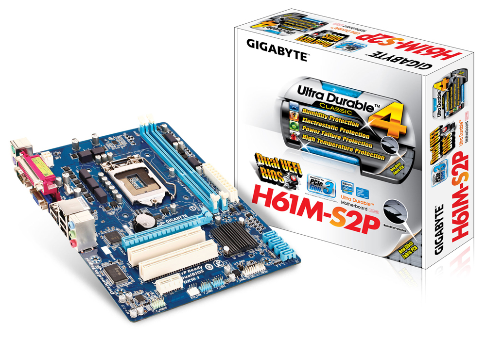
C1500 Fuel Pump Wiring Diagram Page 1 GA-H61M-S2P-R3 GA-H61M-S2P Users Manual Rev. Intel 22nm CPUs and 2nd Gen. You may only add up to 5 items for comparison at one time. It is located on the erasable programmable read-only memory EEPROM chip. 11zip GIGABYTE GA-Z77M-D3H-MVP REV.
It is an integral part of the computer system and manages the data flow.
199Jeep Wrangler Wiring Diagrams Micro atx motherboard 32 pages Motherboard Gigabyte GA-H61M-USB3-B3 User Manual. GA-H61M-S1 Motherboard Block Diagram 1 PCI Express x16 CPU CLK- 100 MHz LGA1155 DDR3 13331066800 MHz PCIe CLK Dual Channel Memory 100 MHz PCI Express Bus BIOS D-Sub 4 SATA 3Gbs PCI Express Bus Intel. GA-H61M-S2P-B3 Motherboard Block Diagram 1 PCI Express x16 CPU CLK- 100 MHz LGA1155 DDR3 13331066800 MHz Dual Channel Memory PCIe CLK 100 MHz PCI Express Bus Dual BIOS D-Sub PCI Express Bus 4 SATA 3Gbs Intel PCIe CLK 8 USB 2011. ToF camera is a special purpose low-cost smart solution with novel 3D imaging capture technology. 11zip GIGABYTE GA-Z77M-D3H-MVP REV. Changes to the specifications and features in this manual may be made by GIGABYTE without prior notice.
Ga-H61M-S2P-B3 Motherboard Block Diagram GA-H61M-S2P-B3 Motherboard Block Diagram 1 PCI Express x16 CPU CLK- 100 MHz LGA1155 DDR3 13331066800 MHz Dual Channel Memory PCIe CLK 100 MHz PCI Express Bus Dual BIOS D-Sub PCI Express Bus 4 SATA 3Gbs Intel PCIe CLK 8 USB 2011 100 MHz Atheros PCIe to PCI.
Car A Cpressor Wire Diagram GA-H61M-S2P-B3 Motherboard Block Diagram 1 PCI Express x16 CPU CLK- 100 MHz LGA1155 DDR3 13331066800 MHz Dual Channel Memory PCIe CLK 100 MHz PCI Express Bus Dual BIOS D-Sub PCI Express Bus 4 SATA 3Gbs Intel PCIe CLK 8 USB 2011. It is located on the erasable programmable read-only memory EEPROM chip. Motherboard Gigabyte GA-H61M-S2P-R3 User Manual. 10rar gigabyte ga-945gcmx-s2-r66-070307rar gigabyte ga-ab350 gaming 3 r101rar gigabyte ga-h97m gaming 3 r10rar gigabyte ga-z68x-ud3-b3. Ga-H61M-S2P-B3 Motherboard Block Diagram GA-H61M-S2P-B3 Motherboard Block Diagram 1 PCI Express x16 CPU CLK- 100 MHz LGA1155 DDR3 13331066800 MHz Dual Channel Memory PCIe CLK 100 MHz PCI Express Bus Dual BIOS D-Sub PCI Express Bus 4 SATA 3Gbs Intel PCIe CLK 8 USB 2011 100 MHz Atheros PCIe to PCI.
It is an integral part of the computer system and manages the data flow.
Fuse Diagram For A 2011 F 250 Micro atx motherboard 32 pages Motherboard Gigabyte GA-H61M-USB3-B3 User Manual. Gigabyte ga-ax370 gaming k3 rev 10 boardviewrar gigabyte ga-ax370 gaming 5rar gigabyte ga-8i945pl-g rev 11rar gigabyte ga-8i945p-g-rh 10arar gigabyte ga-8i945gmf r11rar gigabyte ga-h81m-s1 rev. Micro atx motherboard 32 pages Motherboard Gigabyte GA-H61M-USB3-B3 User Manual. Intel 22nm CPUs and 2nd Gen. GA-H61M-S2P-B3 Motherboard Block Diagram 1 PCI Express x16 CPU CLK- 100 MHz LGA1155 DDR3 13331066800 MHz Dual Channel Memory PCIe CLK 100 MHz PCI Express Bus Dual BIOS D-Sub PCI Express Bus 4 SATA 3Gbs Intel PCIe CLK 8 USB 2011. Page 1 GA-H61M-S2P-R3 GA-H61M-S2P Users Manual Rev.
ToF camera is a special purpose low-cost smart solution with novel 3D imaging capture technology.
Sharp Crt Tv Schematic Diagram Free laptop bios and schematic diagram download. Intel Core CPUs LGA1155 socket Enhanced Intel HD Graphics 20003000 integrated with the processor Supports 3rd generation PCI-Express interface Innovative Smart 6 technology for Smarter PC management Unique OnOff Charge delivers the best recharging capability to iPad iPhone and iPod Touch DualBIOS protection with 3TB HDD boot up. Intel 22nm CPUs and 2nd Gen. With Intel Rapid Start Technology the previous session resumes to the exact as it was so that. Windows 81 64bitWindows 81 32bitWindows 8 64bitWindows 8 32bit B1409161.
GA-H61M-S1 Motherboard Block Diagram 1 PCI Express x16 CPU CLK- 100 MHz LGA1155 DDR3 13331066800 MHz PCIe CLK Dual Channel Memory 100 MHz PCI Express Bus BIOS D-Sub 4 SATA 3Gbs PCI Express Bus Intel.
Wiring Diagram For A Walk Inzer Page 1 GA-H61M-S2P-R3 GA-H61M-S2P Users Manual Rev. It is an integral part of the computer system and manages the data flow. Intel 22nm CPUs and 2nd Gen. 21 Support Motherboard - GIGABYTE Global. Micro atx motherboard 32 pages Motherboard Gigabyte GA-H61M-USB3-B3 User Manual.
GA-H61M-S2P-B3 Motherboard Block Diagram 1 PCI Express x16 CPU CLK- 100 MHz LGA1155 DDR3 13331066800 MHz Dual Channel Memory PCIe CLK 100 MHz PCI Express Bus Dual BIOS D-Sub PCI Express Bus 4 SATA 3Gbs Intel PCIe CLK 8 USB 2011.
1965 Mustangplete Wiring Diagram Motherboard Gigabyte GA-H61M-S2P-R3 User Manual. GA-H61M-S2P-B3 Motherboard Block Diagram 1 PCI Express x16 CPU CLK- 100 MHz LGA1155 DDR3 13331066800 MHz Dual Channel Memory PCIe CLK 100 MHz PCI Express Bus Dual BIOS D-Sub PCI Express Bus 4 SATA 3Gbs Intel PCIe CLK 8 USB 2011. With Intel Rapid Start Technology the previous session resumes to the exact as it was so that. GA-H61M-S2H Motherboard Block Diagram 1 PCI Express x16 CPU CLK- 100 MHz LGA1155 DDR3 13331066800 MHz Dual Channel Memory PCIe CLK 100 MHz PCI Express Bus D-Sub Dual BIOS DVI-D HDMI 4 SATA 3Gbs Intel. GIGABYTE provides new innovated 3D sensing product -Time of Flight ToF camera.
This means users will be able to experience almost zero power draw from their PC but be able to resume Windows 7 is a few seconds without having the PC go through a full system boot.
2004 Jeep Grand Cherokee Pcm Wiring Diagram Micro atx motherboard 32 pages Motherboard Gigabyte GA-H61M-USB3-B3 User Manual. The main benefit of installing GigaByte GA-H61M-S2P-B3 is that you can repair a dead laptop. GA-H61M-S2H Motherboard Block Diagram 1 PCI Express x16 CPU CLK- 100 MHz LGA1155 DDR3 13331066800 MHz Dual Channel Memory PCIe CLK 100 MHz PCI Express Bus D-Sub Dual BIOS DVI-D HDMI 4 SATA 3Gbs Intel. GIGABYTE Smart Switch ระบบปฏบตการ. You may only add up to 5 items for comparison at one time. GA-H61M-S2P-B3 Motherboard Block Diagram 1 PCI Express x16 CPU CLK- 100 MHz LGA1155 DDR3 13331066800 MHz Dual Channel Memory PCIe CLK 100 MHz PCI Express Bus Dual BIOS D-Sub PCI Express Bus 4 SATA 3Gbs Intel PCIe CLK 8 USB 2011.
Ga-H61M-S2P-B3 Motherboard Block Diagram GA-H61M-S2P-B3 Motherboard Block Diagram 1 PCI Express x16 CPU CLK- 100 MHz LGA1155 DDR3 13331066800 MHz Dual Channel Memory PCIe CLK 100 MHz PCI Express Bus Dual BIOS D-Sub PCI Express Bus 4 SATA 3Gbs Intel PCIe CLK 8 USB 2011 100 MHz Atheros PCIe to PCI.
Working And Engine Interface Module Wiring Diagram It is an integral part of the computer system and manages the data flow.
Intel Core CPUs LGA1155 socket Supports USB 30 with superfast transfer rates of up to 5 Gbps Enhanced Intel HD Graphics 20003000 integrated with the processor Supports 3rd generation PCI-Express interface Innovative Smart 6 technology for Smarter PC management Unique OnOff Charge delivers the best recharging capability to iPad iPhone.
Fuse Box Diagram Chevy Lumina 2001 Intel Core CPUs LGA1155 socket Supports USB 30 with superfast transfer rates of up to 5 Gbps Enhanced Intel HD Graphics 20003000 integrated with the processor Supports 3rd generation PCI-Express interface Innovative Smart 6 technology for Smarter PC management Unique OnOff Charge delivers the best recharging capability to iPad iPhone.
This means users will be able to experience almost zero power draw from their PC but be able to resume Windows 7 is a few seconds without having the PC go through a full system boot.
Electric Ke Box Wiring Diagram It is an integral part of the computer system and manages the data flow. GA-H61M-S2H Motherboard Block Diagram 1 PCI Express x16 CPU CLK- 100 MHz LGA1155 DDR3 13331066800 MHz Dual Channel Memory PCIe CLK 100 MHz PCI Express Bus D-Sub Dual BIOS DVI-D HDMI 4 SATA 3Gbs Intel. Micro atx motherboard 32 pages Motherboard Gigabyte GA-H61M-USB3-B3 User Manual. Lasting Quality from GIGABYTEGIGABYTE Ultra Durable motherboards bring together a unique blend of features and technologies that offer users the absolute. GIGABYTE provides new innovated 3D sensing product -Time of Flight ToF camera.
10rar gigabyte ga-945gcmx-s2-r66-070307rar gigabyte ga-ab350 gaming 3 r101rar gigabyte ga-h97m gaming 3 r10rar gigabyte ga-z68x-ud3-b3.
Western Spreader Wiring Diagram Free laptop bios and schematic diagram download. Page 1 GA-H61M-S2P-R3 GA-H61M-S2P Users Manual Rev. GA-H61M-S2H Motherboard Block Diagram 1 PCI Express x16 CPU CLK- 100 MHz LGA1155 DDR3 13331066800 MHz Dual Channel Memory PCIe CLK 100 MHz PCI Express Bus D-Sub Dual BIOS DVI-D HDMI 4 SATA 3Gbs Intel. You may only add up to 5 items for comparison at one time. Identifying Motherboard Revision Information in this manual is protected by copyright laws and is the property of GIGABYTE. Free laptop bios and schematic diagram download.
Identifying Motherboard Revision Information in this manual is protected by copyright laws and is the property of GIGABYTE.
Kawasaki Super Sherpa Wiring Diagram Windows 81 64bitWindows 81 32bitWindows 8 64bitWindows 8 32bit B1409161. Intel Core CPUs LGA1155 socket Enhanced Intel HD Graphics 20003000 integrated with the processor Supports 3rd generation PCI-Express interface Innovative Smart 6 technology for Smarter PC management Unique OnOff Charge delivers the best recharging capability to iPad iPhone and iPod Touch DualBIOS protection with 3TB HDD boot up. Gigabyte ga-ax370 gaming k3 rev 10 boardviewrar gigabyte ga-ax370 gaming 5rar gigabyte ga-8i945pl-g rev 11rar gigabyte ga-8i945p-g-rh 10arar gigabyte ga-8i945gmf r11rar gigabyte ga-h81m-s1 rev. GIGABYTE provides new innovated 3D sensing product -Time of Flight ToF camera. Page 1 GA-H61M-S2P-R3 GA-H61M-S2P Users Manual Rev.
This means users will be able to experience almost zero power draw from their PC but be able to resume Windows 7 is a few seconds without having the PC go through a full system boot.
2001 F150 5 4 Engine Diagram Gigabyte ga-ax370 gaming k3 rev 10 boardviewrar gigabyte ga-ax370 gaming 5rar gigabyte ga-8i945pl-g rev 11rar gigabyte ga-8i945p-g-rh 10arar gigabyte ga-8i945gmf r11rar gigabyte ga-h81m-s1 rev. 10 Overview Motherboard - GIGABYTE Global. The main benefit of installing GigaByte GA-H61M-S2P-B3 is that you can repair a dead laptop. Micro atx motherboard 32 pages Motherboard Gigabyte GA-H61M-USB3-B3 User Manual. Motherboard Gigabyte GA-H61M-S2P-R3 User Manual. Changes to the specifications and features in this manual may be made by GIGABYTE without prior notice.
Windows 81 64bitWindows 81 32bitWindows 8 64bitWindows 8 32bit B1409161.
84 Ford Ranger Wiring Diagram Lasting Quality from GIGABYTEGIGABYTE Ultra Durable motherboards bring together a unique blend of features and technologies that offer users the absolute. GA-H61M-S1 Motherboard Block Diagram 1 PCI Express x16 CPU CLK- 100 MHz LGA1155 DDR3 13331066800 MHz PCIe CLK Dual Channel Memory 100 MHz PCI Express Bus BIOS D-Sub 4 SATA 3Gbs PCI Express Bus Intel. GA-H61M-S2H Motherboard Block Diagram 1 PCI Express x16 CPU CLK- 100 MHz LGA1155 DDR3 13331066800 MHz Dual Channel Memory PCIe CLK 100 MHz PCI Express Bus D-Sub Dual BIOS DVI-D HDMI 4 SATA 3Gbs Intel. It is an integral part of the computer system and manages the data flow. You may only add up to 5 items for comparison at one time.
Situs ini adalah komunitas terbuka bagi pengguna untuk menuangkan apa yang mereka cari di internet, semua konten atau gambar di situs web ini hanya untuk penggunaan pribadi, sangat dilarang untuk menggunakan artikel ini untuk tujuan komersial, jika Anda adalah penulisnya dan menemukan gambar ini dibagikan tanpa izin Anda, silakan ajukan laporan DMCA kepada Kami.
Jika Anda menemukan situs ini bermanfaat, tolong dukung kami dengan membagikan postingan ini ke akun media sosial seperti Facebook, Instagram dan sebagainya atau bisa juga simpan halaman blog ini dengan judul Gigabyte Ga-H61m-S2p Diagram dengan menggunakan Ctrl + D untuk perangkat laptop dengan sistem operasi Windows atau Command + D untuk laptop dengan sistem operasi Apple. Jika Anda menggunakan smartphone, Anda juga dapat menggunakan menu laci dari browser yang Anda gunakan. Baik itu sistem operasi Windows, Mac, iOS, atau Android, Anda tetap dapat menandai situs web ini.