Stick Diagram Cmos Inverter - Jika kamu mencari artikel Stick Diagram Cmos Inverter terlengkap, berarti kamu telah berada di web yang benar. Setiap artikel diulas secara mendetail dengan penyajian bahasa yang gampang dipahami bagi orang awam sekalipun. itulah sebabnya website ini banyak diminati para blogger dan pembaca online. Yuk langsung aja kita simak ulasan Stick Diagram Cmos Inverter berikut ini.
Stick Diagram Cmos Inverter. Next to the inverter layout of Figure 35 we list its 13 components most of which can be also found in the schematic and the stick diagram presented in Figure 34. In some cases other signals must be routed over the inverter. This implies that the substrate is of P-type and an N-Well must be etched into the P Substrate. Stick Diagrams Some Rules Rule 4. There should be enough space between them for other circuit elements.
3 6l V6 Engine Diagram Stick Diagrams Some Rules Rule 4. In CMOS a demarcation line is drawn to avoid touching of p-diff with n-diff. Stick Diagrams y VLSI design aims to translate circuit concepts onto silicon y stick diagrams are a means of capturing topography and layer information - simple. In this video I am going to create a stick diagram design out from a CMOS example. Inverters stick diagram is shown at the end. A red color indicates the current layer.
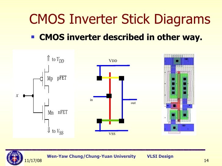
A complementary CMOS inverter is implemented as the series connection of a p-device and an n-device as shown in the Figure above.
2006 Chevy Trailblazer Tail Light Wiring Diagram In the case of CMOS4s we shall be dealing with an N-Well process. Depletion Load Inverter 219201714 kalyan5blogspotin 15. A red color indicates the current layer. Page 2 Manual Design In MicroWind the default icon is the drawing icon shown above. Next Active Green paths must be drawn for required transistors. Stick Diagrams Some Rules Rule 4.
7292018 ECE KU 7 Color Codes Layer Layer Name Metal 1 Polysilicon n-type diffusion p-type diffusion Demarcation line 8.
Shark Nose Diagram Stick Diagram of a CMOS Inverter. 7292018 ECE KU 7 Color Codes Layer Layer Name Metal 1 Polysilicon n-type diffusion p-type diffusion Demarcation line 8. In this video I am going to create a stick diagram design out from a CMOS example. STICK DIAGRAMS UNIT II CIRCUIT DESIGN PROCESSES Examples of Stick Diagrams V out V dd 5V V in V out V dd 5V in. Mask Layout and Stick Diagram for a CMOS Inverter.
Circuits Layout CMOS VLSI Design Slide 7 MOS Integrated Circuits q1970s processes usually had only nMOS transistors Inexpensive but consume power while idle q1980s-present.
98 Chevy K1500 Wiper Wiring Diagram All PMOS must lie on one side of the line and all NMOS will have to be on the other side. In the case of CMOS4s we shall be dealing with an N-Well process. In CMOS a demarcation line is drawn to avoid touching of p-diff with n-diff. Stick Diagrams Some Rules Rule 4. Sketch a stick diagram for O3AI and estimate area. Thus the devices do not suffer from anybody effect.
In this video I am going to create a stick diagram design out from a CMOS example.
1954 Mopar Wiring Diagrams VLSI𝗧𝗼 𝗕𝗨𝗬 𝗻𝗼𝘁𝗲𝘀 𝗼𝗳 𝗦𝗵𝗿𝗲𝗻𝗶𝗸. Layout Stick Diagram of CMOS Inverter 219201713 kalyan5blogspotin 14. CMOS INVERTER STICK DIAGRAM VDD. CMOS VLSI Design Introduction to CMOS VLSI Design Stick Diagrams. LAYOUT OF THE CMOS INVERTER The stick diagram can now be converted into a realistic but still a bit simplified circuit layout presented in Figure 35.
The stick diagrams uses sticks or lines to represent the devices and conductors.
Pressure Level Diagram When you open a window in df II the plane of the screen represents the P-Substrate. In the case of CMOS4s we shall be dealing with an N-Well process. Thus the devices do not suffer from anybody effect. The first two stick diagram layouts shown in Fig. There are many methods in creating this stick diagram so there i. A complementary CMOS inverter is implemented as the series connection of a p-device and an n-device as shown in the Figure above.
Sketch a stick diagram for O3AI and estimate area.
2003 Mitsubishi Eclipse Spyder Wiring Diagram CMOS VLSI Design Introduction to CMOS VLSI Design Stick Diagrams. The palette is located in the lower right corner of the screen. When you open a window in df II the plane of the screen represents the P-Substrate. Euler Paths Peter Kogge University of Notre Dame Fall 2015 2018 Based on material from Prof. This implies that the substrate is of P-type and an N-Well must be etched into the P Substrate.
The schematic diagram of the CMOS inverter with one nMOS at the bottom and one pMOS at the top.
The Kane Chronicles Survival Guide The source and the substrate body of the p -device is tied to the VDD rail while the source and the substrate of the n-device are connected to the ground bus. Jay Brockman Joseph Nahas University of Notre Dame. In the case of CMOS4s we shall be dealing with an N-Well process. Depletion Load Inverter 219201714 kalyan5blogspotin 15. There are many methods in creating this stick diagram so there i. In CMOS a demarcation line is drawn to avoid touching of p-diff with n-diff.
The first two stick diagram layouts shown in Fig.
Crosley Wiring Diagram The stick diagrams uses sticks or lines to represent the devices and conductors. In this video I am going to create a stick diagram design out from a CMOS example. 36 are the two most basic inverter configurations with different alignments of the transistors. Y Transistors y A transistor exists where a polysilicon stick crosses either an N diffusion stick NMOS transistor or a P diffusion. CMOS Inverter 219201712 kalyan5blogspotin 13.
Thus the devices do not suffer from anybody effect.
2003 Buick Lesabre Engine Diagram Cooling Page 2 Manual Design In MicroWind the default icon is the drawing icon shown above. Congratulations you have finished Lecture 13. Stick Diagram of CMOS NAND Gate- Eulers Path 219201716 kalyan5blogspotin 17. In the case of CMOS4s we shall be dealing with an N-Well process. Circuits Layout CMOS VLSI Design Slide 7 MOS Integrated Circuits q1970s processes usually had only nMOS transistors Inexpensive but consume power while idle q1980s-present. Note that there is no difference in the construction of a transistor source and a transistor drain.
7292018 ECE KU 7 Color Codes Layer Layer Name Metal 1 Polysilicon n-type diffusion p-type diffusion Demarcation line 8.
Car Alarm Installation Wiring Diagram Circuits Layout CMOS VLSI Design Slide 7 MOS Integrated Circuits q1970s processes usually had only nMOS transistors Inexpensive but consume power while idle q1980s-present. This implies that the substrate is of P-type and an N-Well must be etched into the P Substrate. GND Fig 6 Connect the source of Pmos to VDD and Nmos to GND CMOS INVERTER STICK DIAGRAM CONTACT. Congratulations you have finished Lecture 13. 36 are the two most basic inverter configurations with different alignments of the transistors.
Layout Stick Diagram of CMOS Inverter 219201713 kalyan5blogspotin 14.
Planning For Love Aisle Bound 1 Sketch a stick diagram for O3AI and estimate area. Next Active Green paths must be drawn for required transistors. B Stick diagram of the CMOS inverter DDV outVinV GND DDV GND inV outV 7. Note that there is no difference in the construction of a transistor source and a transistor drain. Thus the devices do not suffer from anybody effect. Stick Diagram of CMOS NAND Gate- Eulers Path 219201716 kalyan5blogspotin 17.
STICK DIAGRAMS UNIT II CIRCUIT DESIGN PROCESSES Examples of Stick Diagrams V out V dd 5V V in V out V dd 5V in.
Ford Focus Fuse Box Diagram 2009 Cigarette Lighter The schematic diagram of the CMOS inverter with one nMOS at the bottom and one pMOS at the top. Figure below shows the schematic of an inverter. Inverters stick diagram is shown at the end. When you open a window in df II the plane of the screen represents the P-Substrate. Stick Diagram of CMOS NAND Gate- Eulers Path 219201716 kalyan5blogspotin 17.
B Stick diagram of the CMOS inverter DDV outVinV GND DDV GND inV outV 7.
96 Galant Fuse Box Diagram GND Fig 5 Take the output with the poly silicon metal CMOS INVERTER STICK DIAGRAM VDD. Thus the devices do not suffer from anybody effect. A CMOS inverter consists of both P-type and N-type MOS devices on the same common substrate. When you open a window in df II the plane of the screen represents the P-Substrate. In CMOS a demarcation line is drawn to avoid touching of p-diff with n-diff. The palette is located in the lower right corner of the screen.
Figure below shows the schematic of an inverter.
2001 Dodge 3500 Wiring Diagram Y Transistors y A transistor exists where a polysilicon stick crosses either an N diffusion stick NMOS transistor or a P diffusion. In this case A CMOS NAND gate requires two series pull-down NMOS transistors con- nected to. CMOS INVERTER STICK DIAGRAM VDD. CMOS-2 Input NAND NOR GATE 219201715 kalyan5blogspotin 16. 36 are the two most basic inverter configurations with different alignments of the transistors.
Layout Stick Diagram of CMOS Inverter 219201713 kalyan5blogspotin 14.
78 Ford Bronco Wiring Diagram LAYOUT OF THE CMOS INVERTER The stick diagram can now be converted into a realistic but still a bit simplified circuit layout presented in Figure 35. Next Active Green paths must be drawn for required transistors. The palette is located in the lower right corner of the screen. Page 2 Manual Design In MicroWind the default icon is the drawing icon shown above. All PMOS must lie on one side of the line and all NMOS will have to be on the other side. In this case A CMOS NAND gate requires two series pull-down NMOS transistors con- nected to.
In the following we will examine a series of stick diagrams which show different layout options for the CMOS inverter circuit.
Tibia Fibula Diagram Inside The schematic diagram of the CMOS inverter with one nMOS at the bottom and one pMOS at the top. Page 2 Manual Design In MicroWind the default icon is the drawing icon shown above. 36 are the two most basic inverter configurations with different alignments of the transistors. 7292018 ECE KU 7 Color Codes Layer Layer Name Metal 1 Polysilicon n-type diffusion p-type diffusion Demarcation line 8. Figure below shows the schematic of an inverter.
Situs ini adalah komunitas terbuka bagi pengguna untuk mencurahkan apa yang mereka cari di internet, semua konten atau gambar di situs web ini hanya untuk penggunaan pribadi, sangat dilarang untuk menggunakan artikel ini untuk tujuan komersial, jika Anda adalah penulisnya dan menemukan gambar ini dibagikan tanpa izin Anda, silakan ajukan laporan DMCA kepada Kami.
Jika Anda menemukan situs ini lengkap, tolong dukung kami dengan membagikan postingan ini ke akun media sosial seperti Facebook, Instagram dan sebagainya atau bisa juga bookmark halaman blog ini dengan judul Stick Diagram Cmos Inverter dengan menggunakan Ctrl + D untuk perangkat laptop dengan sistem operasi Windows atau Command + D untuk laptop dengan sistem operasi Apple. Jika Anda menggunakan smartphone, Anda juga dapat menggunakan menu laci dari browser yang Anda gunakan. Baik itu sistem operasi Windows, Mac, iOS, atau Android, Anda tetap dapat menandai situs web ini.